264, Naehyangan-gil, Jeongnam-myeon, Hwaseong-si, Gyeonggi-do, Republic of Korea
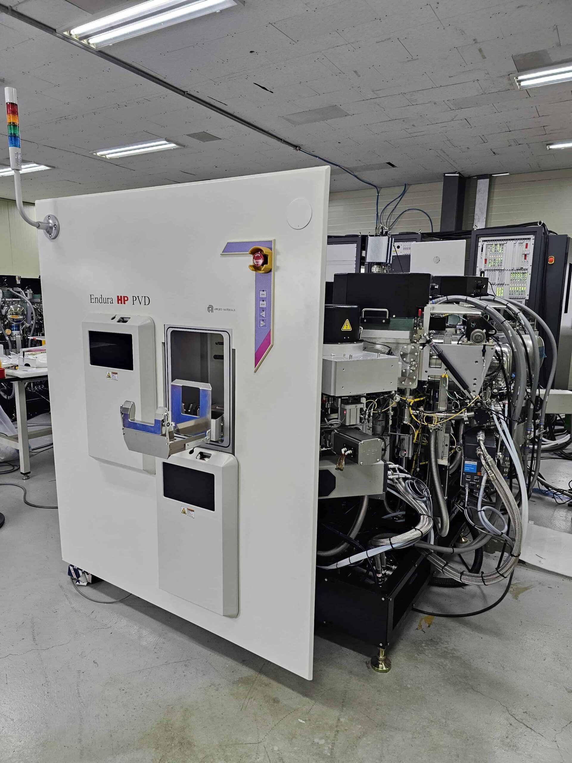
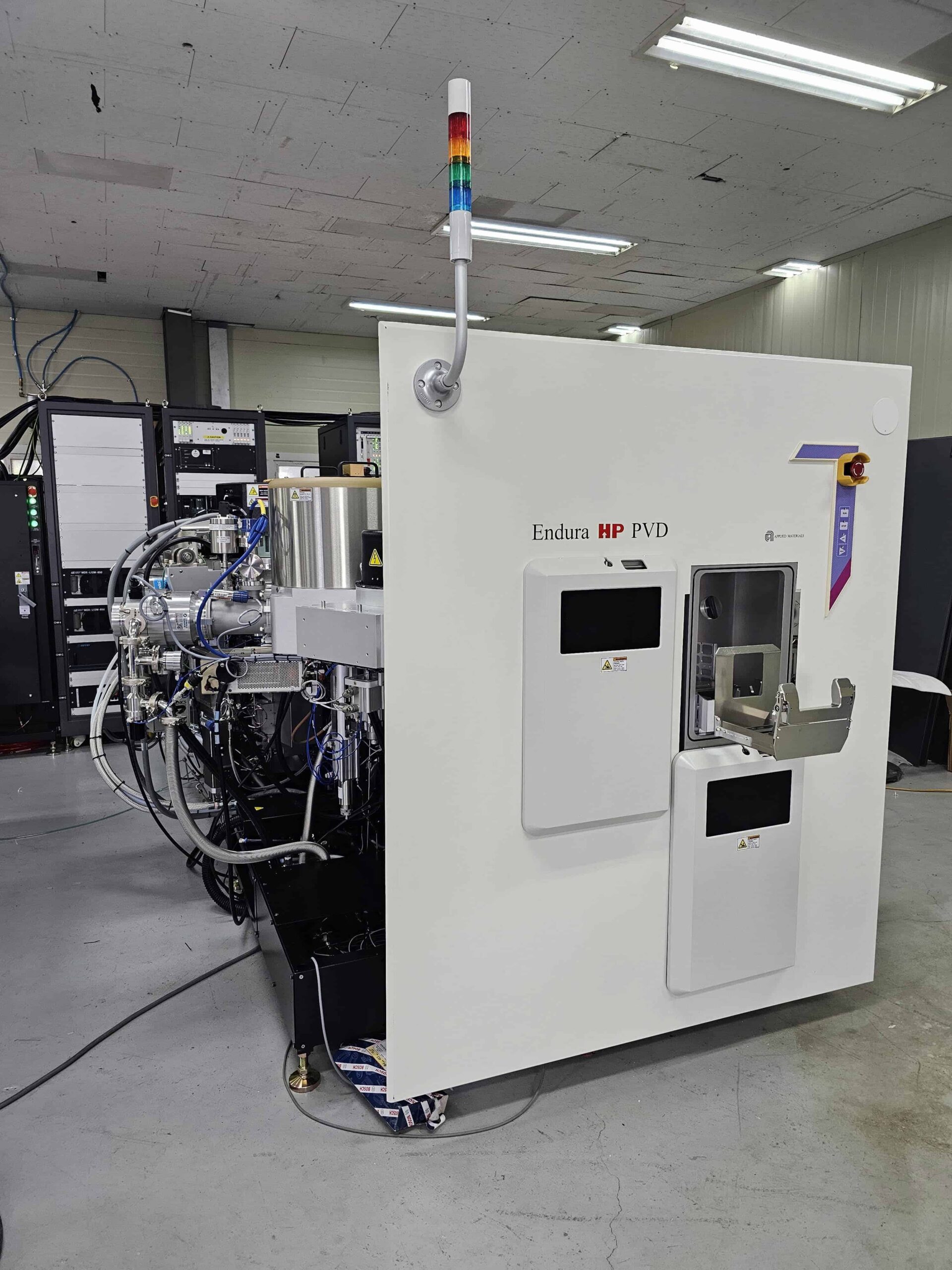
Endura PVD
Endura PVD of Product
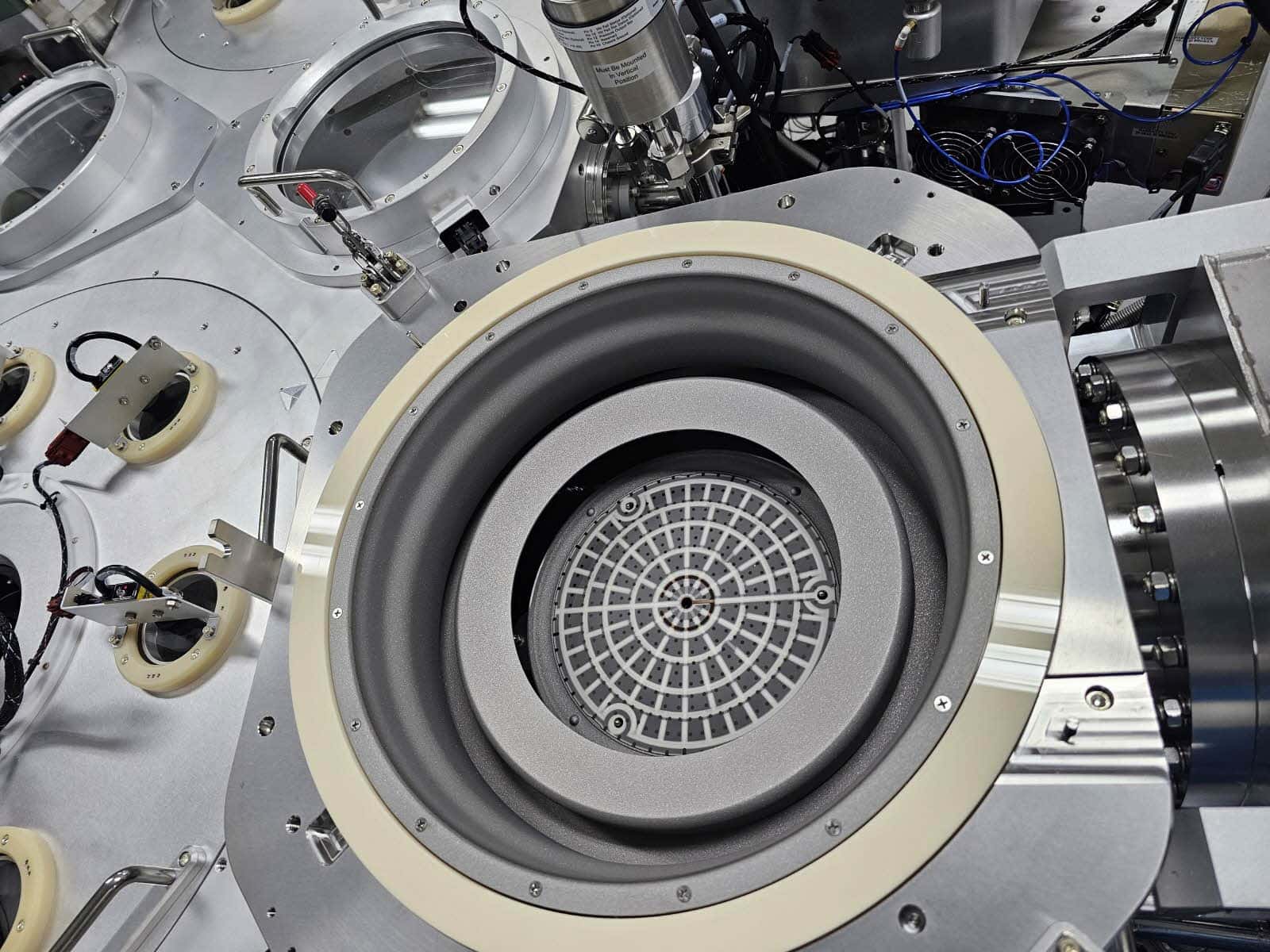
SYSTEM SOLUTION
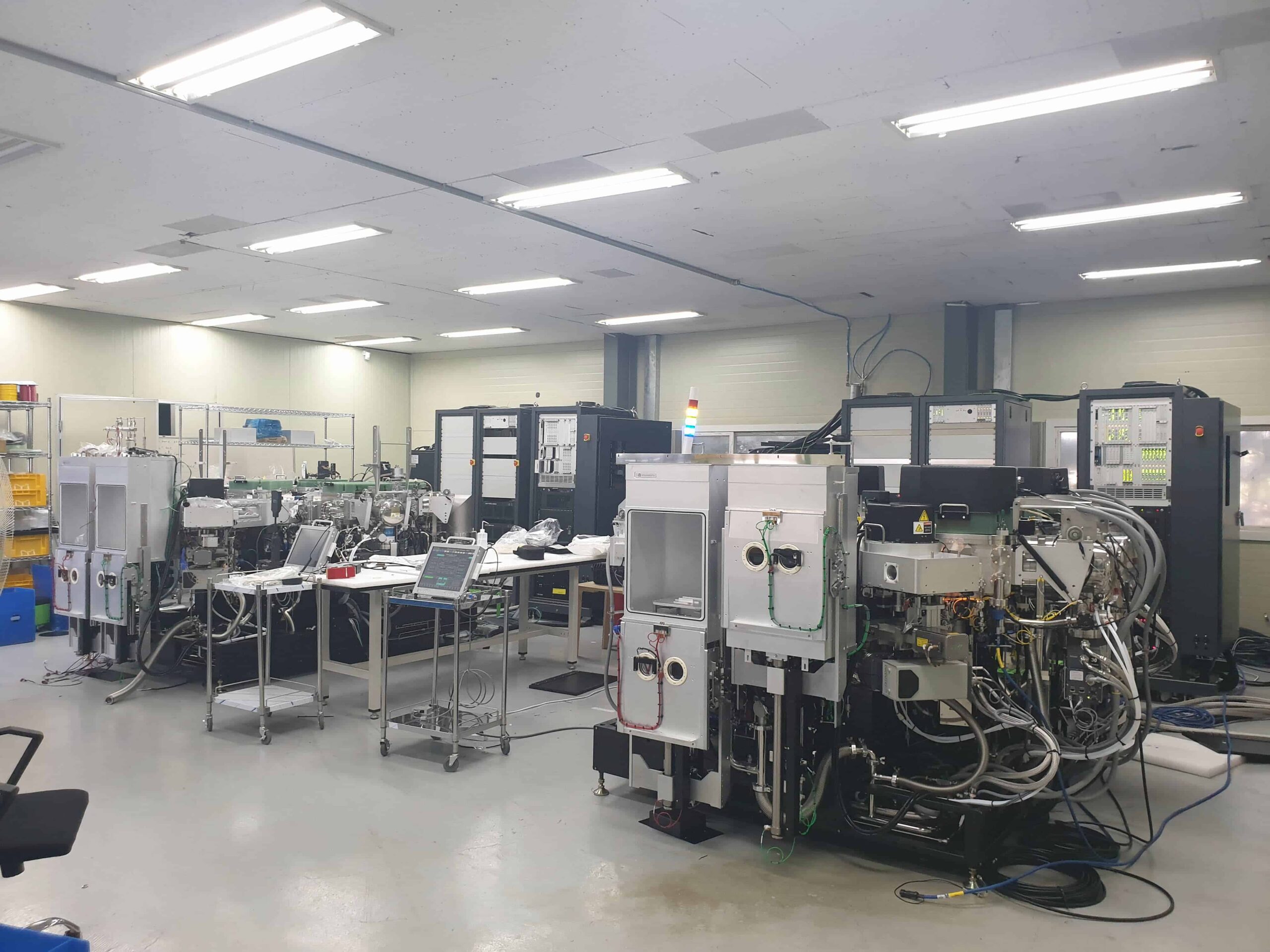
- 5” / 6” / 8” System Refurbishment
- Inch Conversion
- Chamber Addition & Upgrade
- Moved into system another Fab
AMAT 200mm Endura & Centura PVD is the main product, leading the industry’s used equipment based on differentiated technology and know-how, and supplying the best products.
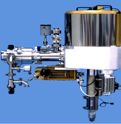
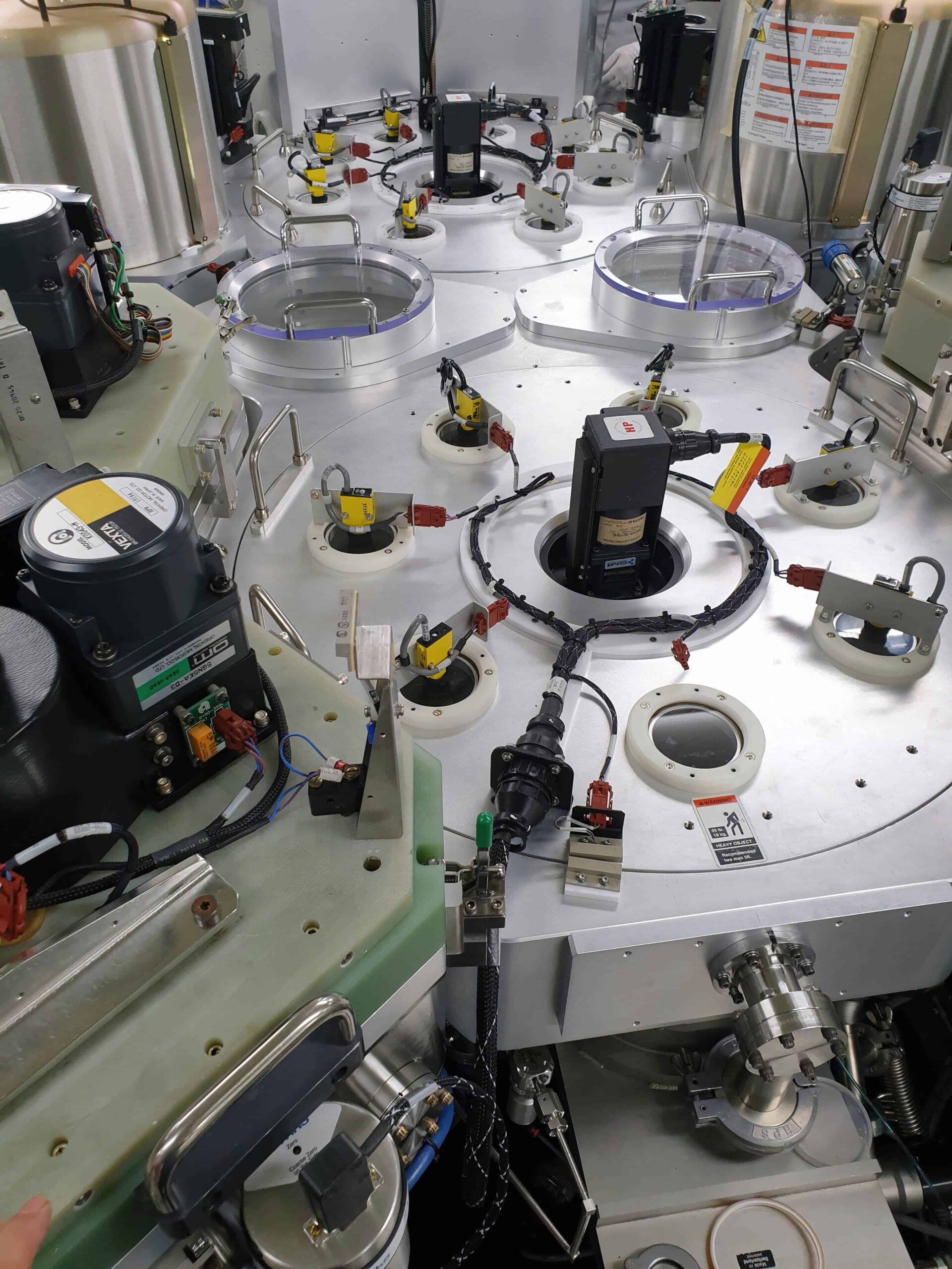
PCⅡ Preclean & RPC chamber
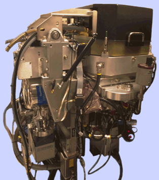
IMP chamber
Ti / TiN
AMAT 200mm Endura & Centura PVD is the main product, leading the industry’s used equipment based on differentiated technology and know-how, and supplying the best products.
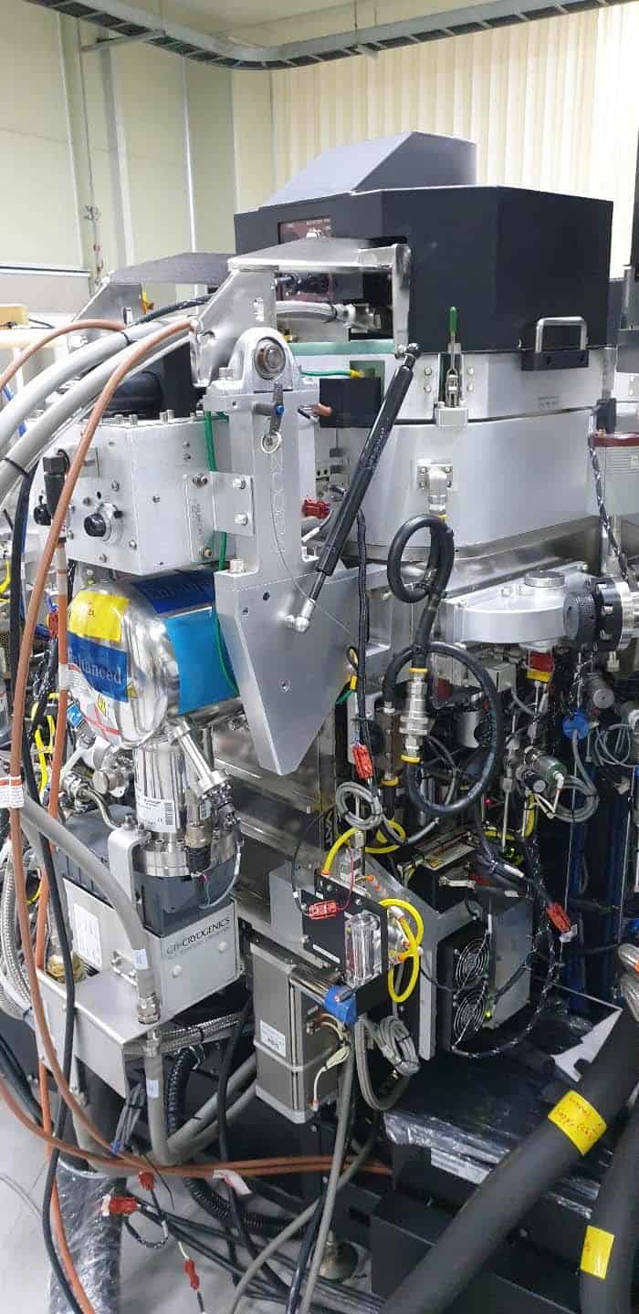
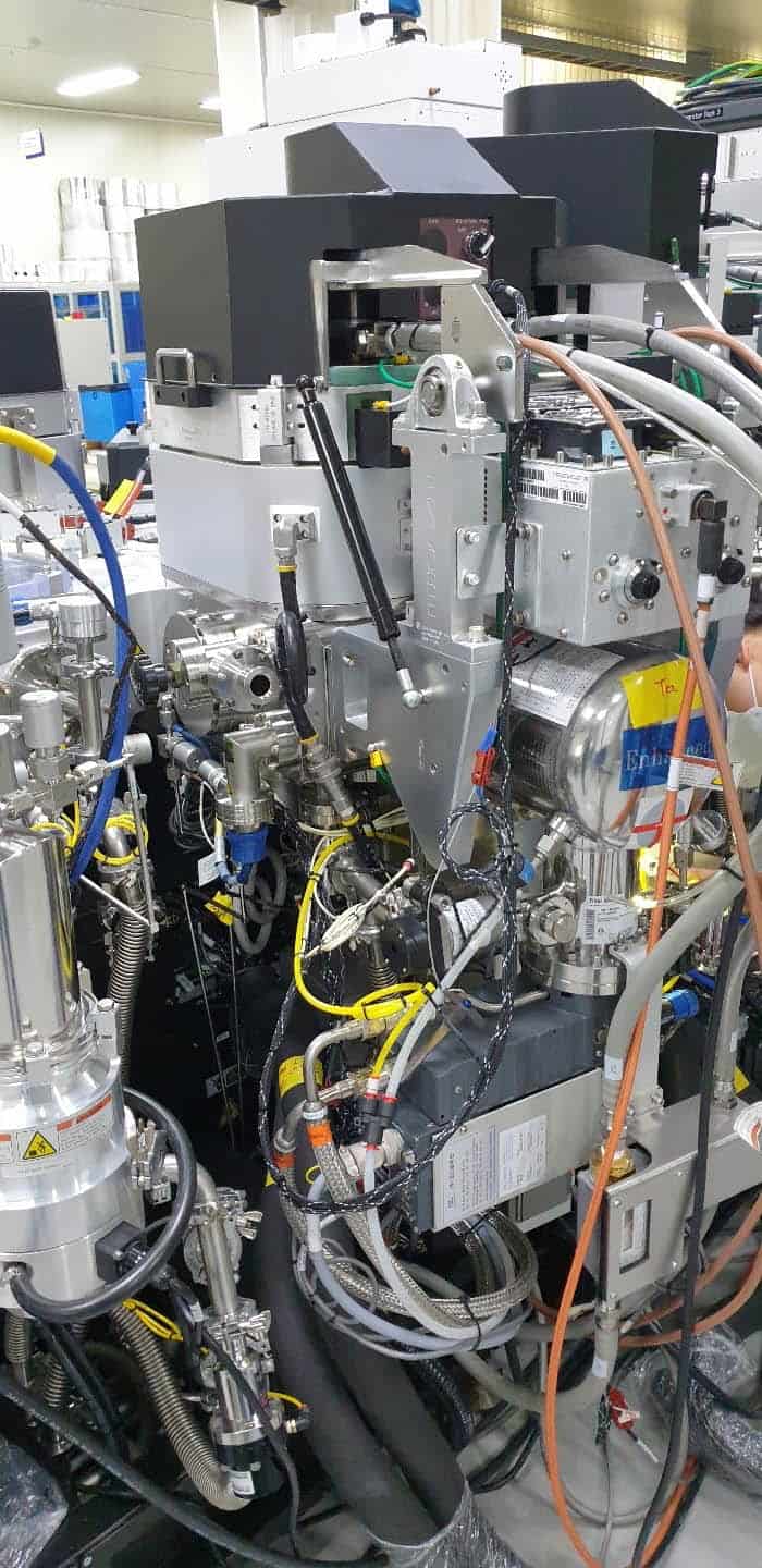
SIP EnCore Cu & Ta/TaN Chamber
AMAT 200mm Endura & Centura PVD is the main product, leading the industry’s used equipment based on differentiated technology and know-how, and supplying the best products.
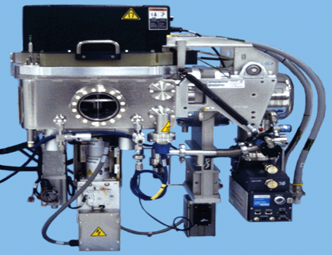
PVD Chamber
HOT Al, AlCu, Ti, TTN, TiW, AlN, SiCr
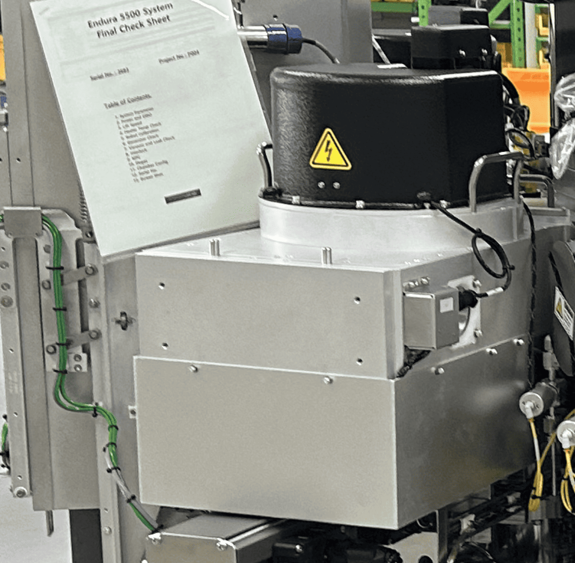
Orient / Degas chamber
STD, Ultra Uniform, Enhanced Temp Feedback
AMAT 200mm Endura & Centura PVD is the main product, leading the industry’s used equipment based on differentiated technology and know-how, and supplying the best products.
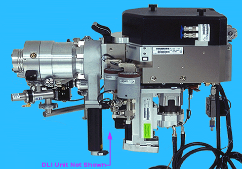
TxZ STD chamber
TiN
TDMAT(Tetrakis-dimethylamino Titanium)
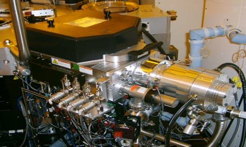
TxZ HP+ chamber
TiN
TDMAT(Tetrakis-dimethylamino Titanium)
AMAT 200mm Endura & Centura PVD is the main product, leading the industry’s used equipment based on differentiated technology and know-how, and supplying the best products.
Endura PVD
Endura PVD systems are physical vapor deposition (PVD) systems manufactured by Applied Materials. PVD is a process used to deposit a variety of films, such as metals, oxides, and nitrides. Endura PVD systems are used primarily for metal metallization in the semiconductor manufacturing process.
Endura PVD Classification
Endura PVD systems are physical vapor deposition (PVD) systems. PVD is a process used to deposit a variety of films, such as metals, oxides, and nitrides. Endura PVD systems are used primarily for metal metallization in the semiconductor manufacturing process.
Process
Metal metallization
- Deposits a variety of metals, such as cobalt (Co), tungsten (W), aluminum (Al), and copper (Cu), to form metal interconnects.
- Used to electrically connect semiconductor devices.
Under bump metallization
- Deposits metal interconnects to electrically connect pads and bumps in the packaging process.
- Used to improve the reliability of the packaging process.
High-performance metallization
- Deposits metal interconnects with high performance, such as low power, high speed, and high reliability.
Deposition technology
Evaporation
- Deposits films by evaporating a source material at high temperatures.
- Has a fast deposition speed and can deposit a variety of films.
Plasma
- Deposits films by ionizing a source material using plasma, and then depositing the ionized source material.
- Can reduce film defects and deposit high-quality films.
Thermal decomposition
- Deposits films by decomposing a source material at high temperatures.
- Has a high film purity and uniformity.
Chamber
Multiple chambers
- Each chamber is designed for a specific process, which helps to prevent cross-contamination between processes and improve film quality.
Single chamber
- Can be used for a variety of processes, which can improve productivity.
Endura PVD Component
Chamber
The chamber is the core component of an Endura PVD system. It is the space where deposition takes place. The chamber performs the following functions
- Supplies the source material for the film to be deposited.
- Deposits the film.
- Cools the deposited film.
Endura PVD systems can be single-chamber or multi-chamber. Single-chamber systems can be used for a variety of processes, which can improve productivity. Multi-chamber systems can be designed for each specific process, which can help to prevent cross-contamination between processes and improve film quality.
Source material
The source material is the raw material for the film to be deposited. Source materials come in a variety of types, including
- Metal source materials: cobalt (Co), tungsten (W), aluminum (Al), copper (Cu), etc.
- Oxide source materials: silicon dioxide (SiO2), aluminum oxide (Al2O3), etc.
- Nitride source materials: silicon nitride (Si3N4), aluminum nitride (AlN), etc.
The source material is an important factor that affects deposition temperature, deposition rate, and film quality.
Deposition device
The deposition device is used to deposit the source material. Deposition devices come in a variety of types, including
- Evaporation devices: deposit films by evaporating the source material at high temperatures.
- Plasma deposition devices: deposit films by ionizing the source material in plasma and then depositing the ionized source material.
- Thermal decomposition devices: deposit films by decomposing the source material at high temperatures.
The deposition device is an important factor that affects deposition technology and film quality.
Vacuum system
The vacuum system is used to remove air from the chamber to improve film quality. The vacuum system performs the following functions
- Removes air from the chamber.
- Maintains the pressure in the chamber.
The vacuum system helps to reduce film defects and improve film uniformity.
Control system
The control system is used to control all of the components of an Endura PVD system. The control system performs the following functions
- Controls the deposition temperature.
- Controls the deposition rate.
- Controls the supply of deposition material.
The control system helps to improve the efficiency and stability of an Endura PVD system.
The components of an Endura PVD system are closely interconnected. Each component affects other components and determines the overall performance of the system.
Endura PVD Features Function
Metal metallization - Endura PVD systems can deposit a variety of metals to form metal interconnects, which are used to electrically connect the various components of a semiconductor device.
Under bump metallization (UBM) - Endura PVD systems can deposit UBMs, which are used to electrically connect pads and bumps in the packaging process. UBMs are important for improving the reliability of the packaging process.
High-performance metallization - Endura PVD systems can deposit high-performance interconnects with low power, high speed, and high reliability. These interconnects are required for high-performance semiconductor devices, such as microprocessors and memory devices.
Versatile film deposition - Endura PVD systems can deposit a variety of films, including metals, oxides, nitrides, insulators, and semiconductors.
High deposition rate - Endura PVD systems can deposit films at high rates, which can help to improve productivity and reduce costs.
High-quality films - Endura PVD systems can deposit high-quality films that can improve the performance and reliability of semiconductor devices.
Support for a variety of processes - Endura PVD systems can support a variety of processes, which can help to improve production flexibility.
Automation - Endura PVD systems offer automation features that can help to improve worker productivity and reduce errors.
Endura PVD Process Description
Metal metallization process
The metal metallization process is an important process used to electrically connect semiconductor devices. Endura PVD systems can deposit a variety of metals, such as cobalt (Co), tungsten (W), aluminum (Al), and copper (Cu), to form metal interconnects. These interconnects are used to connect the various components of a semiconductor device, such as the transistor gates, source/drain regions, and contacts.Endura PVD systems can deposit metal interconnects with a variety of properties, such as thickness, uniformity, and resistivity. The thickness of the interconnects is important for ensuring that the devices have the desired electrical properties. The uniformity of the interconnects is important for ensuring that the devices are reliable and perform consistently. The resistivity of the interconnects is important for reducing power consumption.
Under bump metallization process
The under bump metallization (UBM) process is used to deposit metal interconnects under bumps in the packaging process. These bumps are used to connect the semiconductor die to the package substrate. Endura PVD systems can deposit UBMs with a variety of properties, such as thickness, uniformity, and adhesion. The thickness of the UBMs is important for ensuring that the bumps have the desired electrical properties. The uniformity of the UBMs is important for ensuring that the devices are reliable and perform consistently. The adhesion of the UBMs is important for ensuring that the bumps are securely attached to the substrate.
High-performance metallization process
The high-performance metallization process is used to deposit metal interconnects with high performance, such as low power, high speed, and high reliability. These interconnects are required for high-performance semiconductor devices, such as microprocessors and memory devices. Endura PVD systems can deposit high-performance metallizations with a variety of properties, such as thickness, uniformity, resistivity, and thermal conductivity. The thickness of the interconnects is important for ensuring that the devices have the desired electrical properties. The uniformity of the interconnects is important for ensuring that the devices are reliable and perform consistently. The resistivity of the interconnects is important for reducing power consumption. The thermal conductivity of the interconnects is important for dissipating heat and preventing the devices from overheating.
Maintenance and Management Services
264, Naehyangan-gil, Jeongnam-myeon, Hwaseong-si, Gyeonggi-do, Republic of Korea (18523)
